
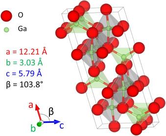
In a groundbreaking study published in ACS Publications, researchers have unveiled a novel approach to enhance the performance of β-Ga2O3-based photodetectors, a vital component in modern optoelectronic devices. The team has demonstrated efficient suppression of persistent photoconductivity through the innovative use of square nanopore arrays. This advancement not only addresses one of the significant challenges facing photodetector technology—unwanted lingering electrical conductivity after exposure to light—but also paves the way for more effective applications in areas ranging from environmental monitoring to advanced imaging systems. As the demand for high-performance photodetectors continues to rise with the proliferation of smart technologies, this latest research offers promising insights into optimizing device functionality and reliability.
Breaking Ground in Photodetector Technology through Nanopore Innovations
The recent advances in photodetector technology, particularly in β-Ga2O3-based devices, showcase the potential of integrating square nanopore arrays to significantly enhance performance. Researchers have demonstrated that these innovative structures effectively suppress persistent photoconductivity, a common issue that hampers the efficiency of photodetectors. By leveraging the unique properties of nanostructured materials, the team achieved a marked increase in responsivity and signal stability, making strides toward more reliable photodetection in various applications. The key findings indicate that the nanopores facilitate better charge carrier dynamics, paving the way for next-generation sensors and imaging technologies.
The implications of this research extend to a variety of fields, ranging from telecommunications to optical sensing. The incorporation of nanopore technologies not only elevates the functional efficiency of photodetectors but also opens avenues for miniaturization and improved integration into complex systems. Key features highlighted in the study include:
- Reduced noise levels: Enhanced signal clarity for better performance.
- Improved thermal stability: Ensuring reliability across various operating conditions.
- Scalability: Potential for mass production without compromising quality.
| Feature | Traditional Method | Square Nanopore Array |
|---|---|---|
| Responsivity | Moderate | High |
| Noise Level | High | Low |
| Temperature Sensitivity | Elevated | Reduced |
Addressing Challenges of Persistent Photoconductivity in β-Ga2O3 Materials
Persistent photoconductivity in β-Ga2O3 materials presents significant challenges for the development of efficient photodetectors. This effect often leads to prolonged conductivity after exposure to light, complicating the device’s response and performance. Recent investigations highlight several key factors contributing to this issue, including:
- Trapping of charge carriers: Photogenerated electrons can become trapped in localized states, prolonging conductivity.
- Defects in the crystal structure: Imperfections can enhance the likelihood of persistent photoconductivity.
- Environmental factors: Humidity and temperature variations can exacerbate the effects of photoconductivity.
To combat these challenges, innovative strategies have been employed, including the integration of square nanopore arrays within β-Ga2O3 structures. This approach enhances carrier mobility while promoting rapid recombination of trapped electrons. Recent experimental results demonstrate a significant reduction in persistent photoconductivity by leveraging this architecture, as summarized in the table below:
| Design Feature | Impact on Photoconductivity |
|---|---|
| Square Nanopore Arrays | Enhances carrier mobility |
| Reduced Trapping Sites | Minimizes conductivity retention |
| Optimized Doping | Improves charge carrier dynamics |
Recommendations for Enhanced Performance in Photodetector Applications
The innovative approach of utilizing square nanopore arrays in β-Ga2O3-based photodetectors has demonstrated a significant reduction in persistent photoconductivity, which is crucial for achieving reliable sensor performance. To further enhance the effectiveness of these devices, it is recommended to focus on the following strategies:
- Optimization of Pore Dimensions: Tailoring the dimensions of the nanopore arrays can lead to improved light absorption and carrier collection efficiency.
- Material Composition: Exploring different doping strategies or composites with other semiconducting materials could enhance the photodetector’s response time and sensitivity.
- Surface Passivation Techniques: Implementing advanced surface passivation can mitigate surface trap states that contribute to persistent photoconductivity.
- Temperature Management: Employing temperature control systems may help in stabilizing the operational state of the devices under varying environmental conditions.
In addition to these recommendations, consistent evaluation of device performance metrics is essential. Here is a summary of key performance indicators to monitor:
| Performance Indicator | Importance |
|---|---|
| Responsivity | Indicates the effectiveness in converting incident light to electrical signal. |
| Quantum Efficiency | Measures the ratio of generated carriers to incident photons. |
| Noise Level | Affects the clarity and reliability of the detected signal. |
Concluding Remarks
In conclusion, the advancements presented in the study of β-Ga2O3-based photodetectors with square nanopore arrays pave the way for a new era of more efficient optoelectronic devices. By significantly suppressing persistent photoconductivity, researchers are not only enhancing the performance of these photodetectors but also addressing a long-standing challenge in the field. As the demand for high-performance photonic applications continues to rise, these findings hold promise for a wide range of industries, from telecommunications to environmental monitoring. The future of photodetection technology appears brighter than ever, driven by innovative designs and a deeper understanding of material properties. As the scientific community continues to explore and refine these developments, we can expect to see even more breakthroughs that will shape the future of light-sensing technology. Stay tuned to our coverage for more updates on this fast-evolving field.